RIO Developer Essentials Guide for Academia
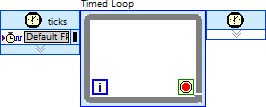
"Single-Cycle Timed Loop" element
Make your first FPGA application
FPGA procedure
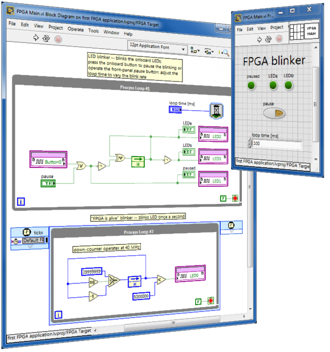
Follow along with this step-by-step tutorial to make a "hello, world!"-like application to experience the advantages of multiple linked VIs running simultaneously on the FPGA target, real-time (RT) target, and desktop computer: (1) "FPGA Main" VI blinks the onboard LEDs and reads the onboard button; these onboard devices physically connect to the FPGA I/O pins, (2) "FPGA testbench" VI runs on the desktop computer for interactive development and debugging of "FPGA Main" in simulation mode prior to compiling to a bitstream file, (3) "RT Main" VI runs as the RT target start-up VI; it runs "FPGA Main", interacts with its front-panel controls/indicators, and communicates with an external desktop computer via network-published shared variables, and (4) "PC Main" VI runs on the desktop computer as a user-friendly human-machine interface (HMI) for remote command and control of "FPGA Main" through the network.
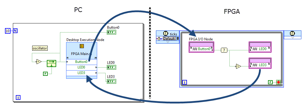
"Desktop Execution" node as an FPGA VI testbench
FPGA code PC code
The PC VI interacts with the FPGA VI in simulation mode to apply a test sequence as the FPGA VI input and monitor the resulting output sequence.
Derived clock domains
FPGA code
Use a derived clock domain to effectively speed up or slow down the FPGA's 40-MHz clock for a selected portion of the FPGA block diagram.
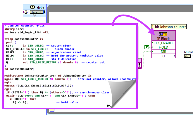
Reuse existing and validated VHDL-based circuit functionality in the FPGA block diagram instead of developing new LabVIEW G code to implement the same functionality.
Xilinx IP integration
FPGA code
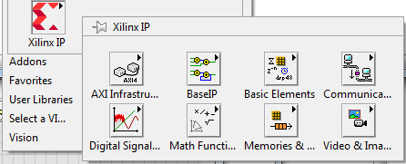
Configure and use Xilinx IP (intellectual property) modules designed specifically for the Xilinx Zynq FPGA
Local variable (FPGA)
FPGA code
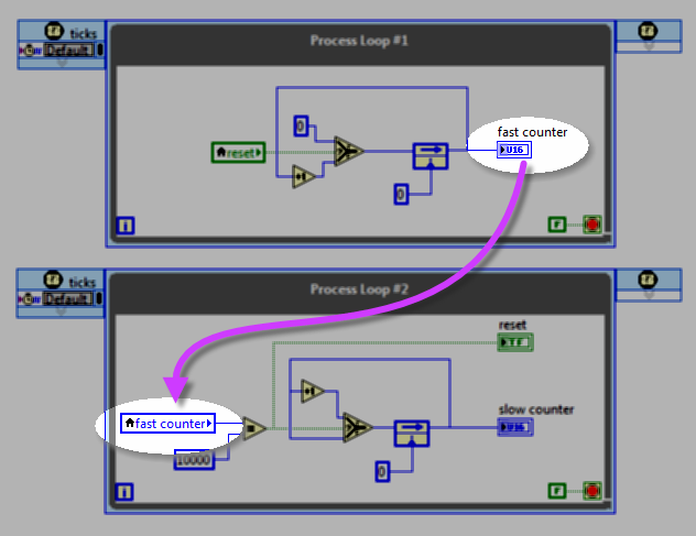
Use a local variable (front-panel indicator) to communicate between two parallel process loops contained within the same VI.
Global variable (FPGA)
FPGA code
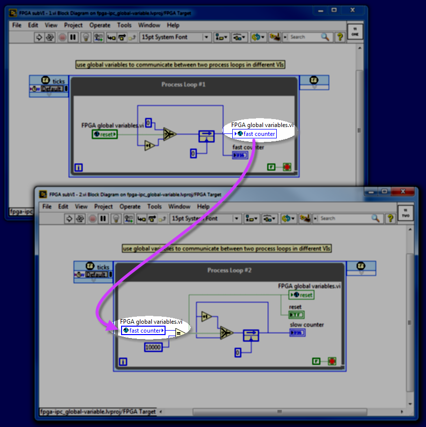
Use a global variable to communicate between two parallel process loops contained within different VIs under the same target.
